2.4.2. Basic Computer Logic Circuits |
The development of digital computers is closely associated with the development of technology of integrated circuits, which provides innumerable possibilities for creation of compounds logic circuits in a single enclosure very small volume.
To the inputs of logic integrated circuits lead to impulses over which we want to execute logical operations, and the result of the operation can be seen at the exit immediately after the input condition or the extent permitted by managed a clock generator.
|
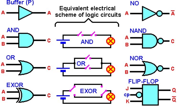
| Figure** 2.4.2 Basic logic circuits of computers / NAND circuit. ( + / - ) |
Compared with the truth tables in the previous chapter, the only circuit that does not perform a logical operation BUFFER. Its task is to carry the state with the input to the output without change, and the way to create electronic logic circuits, which are basically a group of boosters, is able to regenerate the input pulse if it came distorted, and acts as a check valve, one way miss signal The second direction is not to be missed as a router traffic. For this type of action can not be said that the logic circuit acts as a rectifier. One could argue that it serves to separate (separation) or direct sequence impulse.
The above shows that each gate besides performing logical operations also has a regenerative function regarding the form of pulses. Linking logic circuits into a single functional unit accomplished individual tasks as well as other arithmetic operations. In Figure 2.4.2b shows that in the very beginning of a set of logic circuits designed in the bipolar TTL (Transistor-transistor logic) technology installed in standardized plastic casing and Figure 2.4.2c shows the wiring diagram 'NAND' logic circuit . Incidentally, circuits for civilian use had 7xxx label, and assemblies for military use 9XXX tag. Of course, the main difference is in the temperature range of deviation from the needy and parameters.
More integrated transistor units in a single functional unit, installed in a common enclosure, forming INTEGRATED CIRCUIT, called in popular CHIP. Nowadays almost TTL technology is not used, it is possible to find integrated circuits, as shown in Figure 2.4.2b, but the CMOS (Complementary Metal Oxide Semiconductor) technology development and usually have a label 4XXX and 5XXX. CMOS technology is used unipolar transistors which are characterized by a much lower power consumption, size, and performance, and are used with smaller casings. Making integrated circuits, such as the circuit in Figure 2.4.2b, the quantity is much smaller than in the era of application TTL technology.
Today's integrated circuits contain many more elements than transistor used, and their logic functions are much more complex and multifaceted, often have therefore made strictly as a dedicated integrated circuit in accordance with the requirements and needs, rather than as a set of general purpose (design according to requirements - custom design ), and is increasingly integrated circuits that are designed strictly dedicated, assemblies such as graphical support, binary computing and control, analog signal processing, converting an analog signal into a binary sequence of pulses and make a variety of complex tasks. Former receiver the size of a shoe box, is now basically implemented on a single integrated circuit the size of a few millimeters, which assists low-noisy input pair of transistors for receiving HF signals from an antenna and of course the power amplifier to the speaker, which again is an integrated circuit for amplification of NF analog signal output from the receiver. One of the products of such features is a very popular MOBILE PHONE. More space occupies its battery, the screen and keys, but the electronic circuits that are built into it.
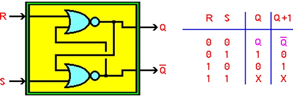
The icons in Figure 2.4.2 and 2.4.2b are rooted in the Anglo-Saxon medical literature, although they may encounter and different but similar names. But to illustrate the labeling and drawing logical circuitry are sufficient examples of the image. From basic logic circuits can be designed and complex logic circuits that will be in the computer behave as adjusters, routers, traffic data, operational data store (registers), and one of the main complex device is flip-flop (flip-flop), logic circuit that is in a state by state excitation remember until the next excitation. The simplest circuit is a ' RS ' flip-flop is shown in the following Figure.
|
| Figure* 2.4.3 Logical diagram and truth table of RS flip-flop. ( + / - ) |
Flip-flop has two inputs and two complementary outputs. 'S' (set) compared to the input that at its opening (bringing the logical value of '1') setting out 'Q' to '1'. 'R' (reset) when the action set out 'Q' to '0'. The truth table output state of flip flops before a change is indicated by 'Q', a condition caused by changes indicated by 'Q +1'. The inputs can result in four different binary combinations as shown in the truth table with a combination of '1-1 ' is not allowed because the outcome is uncertain (marked 'X'). The combination of inputs '0-0' means that the current output state reserves. Figure 2.4.3 shows that the state version of flip flops at the output changes immediately after the presence of the state at the entrance, while Figure 2.4.3b shows that the state version of flip flops at the output changes according to conditions at the entrances but only in the presence of the control pulse (cp) from the clock generator. Supervising the operation of the generator clock synchronized to perform multiple logical operations, or their simultaneous 'parallel' operation. As the third clock control input parameter, in this case, truth tables should have eight lines, in his state of '0' and '1'. But the state of belonging 'zeros' are of no significance during operation flip flops because nothing is changing, and therefore the truth table is not extended for another four rows.
Uncertainty in the states at the output is not a stable feature of the work is from the ' RS ' flip flops developers ' JK ' flip-flop that is missing, namely a combination of '1-1' at the entrance means changing the output state to the opposite value of previously existing conditions, and its principle and realization of the truth table is shown below.

|
| Figure 2.4.4 Logical diagram and truth table of JK flip-flop. |
What they all referred to the situation with output ' Q ' returns the input that activity based belongs to the opposite door, and that positive feedback between the output and input which has a special feature that enhances-supports the change that was made. The same applies to the complementary output. Because of this change in status of these logic circuits performed tremendously fast and this principle is used in making high-speed working memory. Besides these basic types of flip flops are derived others, such as devices for recording delays and the like. If the feedback resistor and capacitor elements can be implemented in clock generators, and the use of quartz crystals can be achieved very high stability of the operating frequency.
Example I
Realization of summation binary numbers in a computer:
|
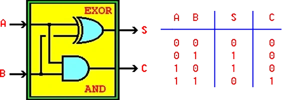
| Figure 2.4.5 Logical diagram and truth table of half-adder. |
The circuit in the Figure above only performs addition operation without transmission shown in output 'C'. The circuit will perform the task for the zero bit binary number (the first digit). To transfer included when adding the next bit of the binary number (for further digits) means that the output of 'C' must join inputs 'A' and 'B' for each subsequent digit or one half-adder exercised to add binary digits, and the second to calculate the sum to be added the previous transmission and so for each the next digit.
If the last digit in summation appeared overflow, it would be stored in the status register (container) microprocessor and user make this phenomenon signaled in mind any messages.
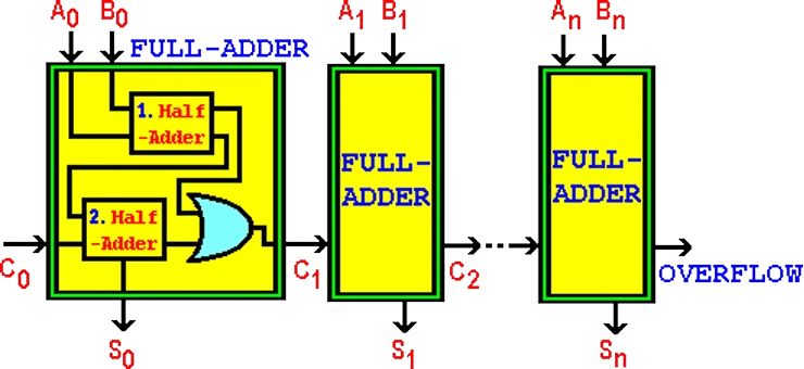
Half-adder in Figure 2.4.5 performs the addition operation only two bits. To transfer included when adding up the bits higher weight takes three inputs. This means that the full adder consists of two half-adders one of which performs binary addition, a second transmission that gets added to the previous adder. One possible realization adder is shown in the following Figure.
|
| Figure 2.4.6 Realization of full-adder for binary numbers 'A' and 'B'. |
'A0' and 'B0' are the least significant bits, and there is no need to input 'C0' leading broadcast. Result of the addition is the 'S0'. The other two bits numbers 'A' and 'B' are coming to the inputs 'A1' and 'B1', and transfer 'C1' to the input of another full-adder. The first half-adder of second adder are summed binary digits 'A1' and 'B1', and their sum is added to the second half-adder transmission 'C1' ("1" or "0", depending on the outcome of the calculation). Result of the addition is the 'S1', and transfer 'C2' going to the next full-adder. OVERFLOW formed during summation is stored in STATUS register of microprocessor.
Number corresponds to the number of full-adder bits binary numbers 'A' and 'B' with which performs calculations. Input of all bits the same time, and therefore for such a binary adder (binary adder) says that performs PARALLEL addition.
Adder is a very important digital computer logic circuit due to the fact that all the mathematical operations ultimately boil down to add binary numbers as described in Chapter 2.3. There are realizing adder for summing series of binary digits (bit by bit), which is due to the slowness in processing the data is often not used.
Example II
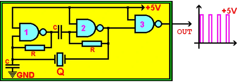
Clock derived from the logical NOR circuits:
|
| Figure 2.4.7 Clock generator realized logic circuits. |
TTL logic circuits manufacturing technology is one of the first to enable the development of efficient integrated circuits. In its early stage technology with one simple integrated circuit contained for example four NOR circuit in one case, as the Figure 2.4.2b, of which three in this case used as in Figure 2.4.7. The power supply is +5 V (Vcc) relative to ground (GND). Resistors R serve as a negative feedback loop between the input and output logic circuits with regard to achieving stability in their individual work, and quartz crystal 'Q' as 'LC' component is a positive feedback loop between the first two sequentially related or logic circuits. +5 V at one of the entrances displayed 'NO' assemblies means that these inputs are always in a state of "1". TTL integrated circuit with four NI assembly is also made of several transistors, resistors and diodes per NI assembly (Figure 2.4.2c) and he is fourteen feet that were connected to running power and ground, and entrances and exits eaten separated NI assemblies. Linking assemblies being made the wiring outside the case. Long since this technology is not used, but the principles of the use and functionality of the logic circuits have not changed.
Example III
Realization of binary counter:
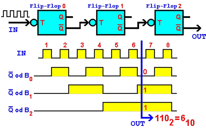
One of the basic combination of logic circuits in digital technique is pulse counter. His next task is binary counting and division frequency. The basic element is a flip-flop counters. The simplest example performed with ' T ' flip-flop is shown in the following Figure.
|
| Figure 2.4.7 Asynchronous binary counter. |
The ' T ' flip-flop has the property, according to performance in the picture, it changes the state of the output at each crossing of input pulses from a state of "1" to "0" state. If the output from one flip flops used as input to other than the effect of sharing frequencies, you see the pulse length on each of the outputs, binary combinations of the outputs of flip flops just give the binary value of the number of pulses that are newcomers to the entrance to the meter.
Timer with three flip-flops to count to 23 = 8. With a large number of flip-flops and a collaborative one with exit to the entrance of one of the past can be achieved by counting to ten.
Counters have a particularly great importance in the design of electronic components for measurement purposes. And only a digital computer in design contains several meters of which the work of one of them recognize the date and time display on the PC monitor.
SUMMARY:
Logic circuits are connected in a variety of functional units are an integral part of the computer and its auxiliary devices. Development of logical circuits and logical design units is closely related with the development of technology that is intended to be general in the small volume placed as more logic circuits and their speed of operation which is greater. Such a set of circuits, located in a common casing with bushing to connect with the environment, popularly called the INTEGRATED CIRCUIT - 'CHIP' (slang - cockroach), and often containing thousands of logic circuits that perform various INSTRUCTIONS provided PC speed up to one hundred million instructions in second (100 MIPS).
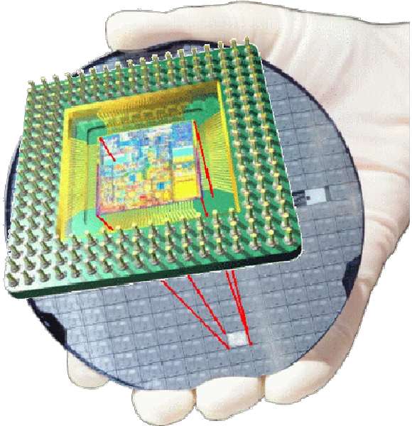
Technology development is based on the development of a group of hundreds of identical integrated circuits at once. At a basic background cut out of monocrystalline silicon (wafer) with various etching and electrochemical methods steaming different materials and their thermal processing is used for the electronic circuits. Illuminated 'rectangle' in Figure 2.4.9 is a one of a multitude of identical circuits with some discs. When the 'rectangles' gets broke into discrete units to be installed in a casing with gold pins and connections associated with the pin contact assembly casing. Before installing the casing tested for accuracy, and then another one when mounted in the casing. As all 'rectangles' are not in the same place in a pie is better 'baked' and show better performance during operation. When testing some permanent damage. Those who have passed the tests of the same charge more 'brothers' who eventually passed the tests without damage but does not meet the required criteria to the full extent. Therefore the different means, for example 'Pentium®4 3.6 GHz' and 'Pentium®4 2.8 GHz', but differently priced.
|
|
| Figure* 2.4.9 Creating a 'wafer' with integrated circuits. ( + / - ) |
The technology of making integrated circuits - MICROELECTRONICS, is a determining factor in the development, manufacture and design of computer systems of tomorrow. The basic premise is that of microelectronics in fewer places to put as many electronic components, which are the integration of the individual will get a different logic circuits, which in turn integrated into a single functional unit can perform their intended tasks.
Size of each component depends on the characteristics of materials used, the manner of their technological processing, anticipated operating frequency (clock speed) and quite a few other factors. Generally referred to micro and nano meter technology, for example a microprocessor in 90 nm and 45 nm technology or memory in 30 nm technology and the like. These Figures are basically reached the limits to reduce the size of elementary transistors embedded into logical units of integrated circuits (chips), which are called according to usage operative amplifier, power amplifier, a microprocessor, a graphics processor, chipset, memory chip, and the like.
It is incontestable that in our daily life computer omnipresent, from the cooling system, the machine on, and all of us in order to facilitate the daily tasks. Pursuant to the growing penetration of microelectronics, life rhythm is faster man all you need not have any positive effects. What the future will show.
|
Citing of this page: Radic, Drago. " Informatics Alphabet " Split-Croatia. {Date of access}; https://informatics.buzdo.com/file. Copyright © by Drago Radic. All rights reserved. | Disclaimer |