Chip - Integrated Circuit - Cooling |
Chip is the most complex achievement of modern microelectronics, or more integrated circuit manufacturing technology. Basically it is a set composed of electronic components in a way to perform actions with a dedicated analog or digital signals. In computer technology is strong digital signal processing in a way to carry with them a variety of logical operations in the binary system of numbers for calculating complex mathematical tasks that the end result is to get the desired result either as a set of numerical data that will be used for some sort of analysis or as the data that would be used 'build' graphic on screen user-friendly man. These products are typically in the application of general dedicate called CPU (Central Processing Unit), FPU (Floating Point Unit) and the GPU (Graphics Processing Unit) or the ChipSET (group of chips - a set of integrated circuits for the purpose of coordinating the system). If it is a special version for users with custom designs for specific dedicate - ASIC (Application Specific Integrated Circuits) such integrated circuits can contain all of the above products generally dedicate a greater or lesser extent.
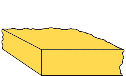
No matter what it is it is a complex technological process, which implies that the surface area of a few square millimeters photo process, etching and vapor deposition of various materials in high vacuum, using for this purpose, made masks, gets layered structure after thermal processing behaves as a transistor, diode, resistor, capacitor or plain connecting cable. Principal way of making elementary transistors by the lithographic process, one of tens of millions of interconnected electronic elements on the said substrate is shown in the following figure.
 |
|
| Figure* 1. Principle of making transistor of chip. |
The Figure shows an elementary transistor in a single layer. When making and mutually connect a multitude of them, in millions, in multiple layers, each element performs some function, then all together reminders to hamburger, only whole of 'sandwich' is not for eat :-).
Description of individual layers and presented the way they work after chemical and thermal processing is too complex to be briefly described and the alphabet is not an issue, but it is striking that the size of the presented element is a pair of tens nm and that by consolidating obtain a set of tens and and hundreds of millions of electronic elements that are capable of performing highly complex logical operations on the principles of the binary number system. The smaller size of elementary transistor with improved technology insulator between the layers, the higher the density of embedded components per unit area, or better yet, a number of active logic elements and substantially less HEATING of the entire chip.
It defines the size of the elementary transistors used at production technology type, from the Intel 4004 microprocessor developed in 10 µm technology (1971), and the Pentium 4 microprocessor developed in 90 nm technology (2005) to the Core series of microprocessors manufactured in 45 nm technology (2007), 32 nm technology (2010), 22 nm technology (2012) and 14 nm technology (2015). DRAM memory is actually being produced in 20 nm technology, and presented examples of graphics processors that follow this trend towards the 16 nm and 12 nm technology (2017). The ARM processors, which are mostly used by mobile devices, are manufactured in 10 nm technology. As the same time does not make one small plate, but the mask is designed so that both can make hundreds of them on a large surface as shown in Figure 2.4.9, the price of these products every day is getting smaller. First performance logic circuits were based on the use of bipolar transistors and used a TTL (Transistor-Transistor Logic) concept development designed 60's. Shown in the animation shows the principle of making just one bipolar transistor PNP or NPN type on which the design was based TTL technology. This technology almost completely replaced the CMOS (Complementary Metal-Oxide-Semiconductor) based on the concept of a unipolar transistor, characterized by a very large resistance to noise, small power consumption and significantly smaller size of the elementary type PMOS or NMOS transistor analog to TTL technology. Almost all electronic computer circuits in this millennium, a microprocessor, microcontroller, RAM and other digital logic circuits based on the use of some version of CMOS technology.
Cutting boards of 'wafer' (cake) into elementary components are obtained elemental integrated circuits (the die), which are tested before cutting to the core functionality, and by cutting and destroying defective correct, setting chip in the casing (the package) in which by golden threads chip is connected with pins of casing. The result is an integrated circuit - chip. Integrated circuits for mass production of miniature devices such as wristwatches and electronic toys directly compose the printed board without casing, such as by addition of smaller size and lower price is achieved.
How are all the chips in the 'wafer' can not be fully dealt with in the same way, some of them will be defective and will be part of the 'wrong baked' and will therefore have a poorer performance than the correct 'brothers'. Based on the results of the final tests of the finished product, the chip is inserted into the casing, defines a series of products. During the final test of them burned out, compensating for the increased cost of products that provide the best performance. Thus, the microprocessors that run at a frequency of 2 GHz and microprocessors that run at a frequency of 3 GHz, the result of the same manufacturing process but during processing were not in the same place in the 'wafer' and possibly even in the same 'wafer'.
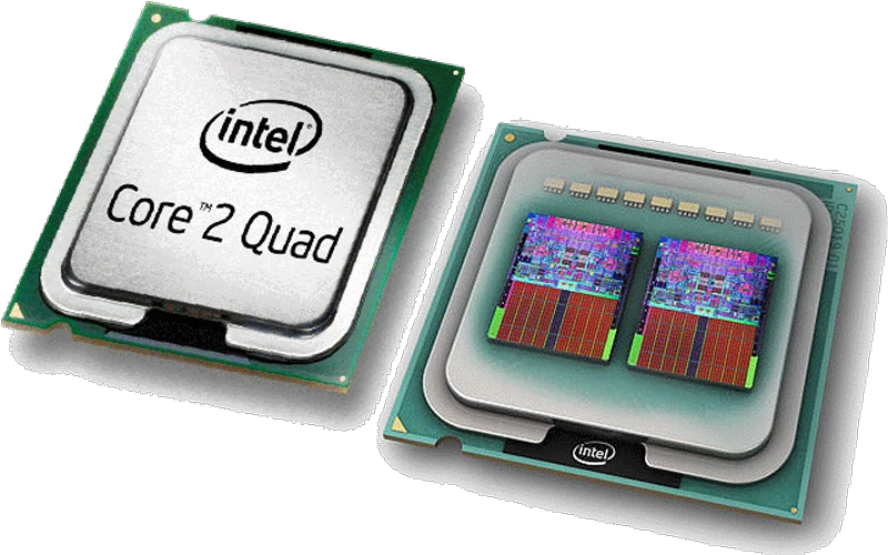
Surely the most popular product of a microprocessor - the CPU, which is often taken as a measure of the effectiveness of computer systems, although its share without compliance with other components of the computer system does not have great significance. A powerful microprocessor in the computer that still has not been resolved cooling, plenty of RAM, disk devices fast enough and large enough bandwidth bus system will not come up. In the following figure shows the cross-section of the casing and one of the popular company INTEL processors.
|
| Figure* 2. Advertising firm views of microprocessor by INTEL. ( + / - ) |
Time requirements imposed by the new criteria in the design of microprocessors. Inability to increase the clock speed due to severe reduction processing the elementary dimensions of transistors, resulting in designs with multiple processor cores, and the previous figure can discern that the design includes two microprocessors with doubled cores giving four cores. Cache of microprocessor (L2 Cache) in the example are separated by cores and can be compiled for all cores. It can be expected that further development of microprocessors go exactly in the direction of making processors with multiple cores with the aim of simultaneous processing of multiple processes, and adding Cache (L3 Cache), which will integrate their communication to the working memory. Graphics processors with their particular tasks follow this trend.
For comparison with the technologies of the last ten years, it is interesting to note that the L3 Cache is incorporated into the motherboard in the form of fast SRAM memory standard sizes 64, 128, 256 or 512 kB, which is largely determined price motherboard and system performance in general. This concept has ceased to be used when the technological development of the microprocessor made possible the increase of its L2 Cache to the extent that they are lost in the system's performance. Integration into the microprocessor L3 Cache revives onetime concept to a new more efficient way. One example is the original conception of microprocessors 'Intel Core i7', which is mounted in a socket type LGA 1366, and by connecting with peripherals just 1366 connections. Casing integrated circuit is not standardized for products like this, but the casing and connectors integrated circuits generally dedicate usually are as shown in Figure 2.4.2b.
The increasing use of virtual machines is likely to affect the described design of integrated circuits to the available resources as far as possible evenly. One of the display processor in the figure above shows that for the connectors used are oval footer of connectors (pins) instead of pins as shown in Figure 2.4.9. Most pins function is unified so that one is used to power the pin group, the ground and other similar facilities, in order to ensure that in the event of poor contact of the one pin has a second full functionality. Moreover, the studies have shown that oval connectors have a lower percentage of unrealized contacts compared to the previously used the base with the 'needles'.
Interworking function properly diverse group of chips on the motherboard of your computer and insert the card and their proper interpersonal communication, such as CPU, GPU, working memory, disk and optical devices, chip for music, support chip for network support, and others is responsible CHIPSET, basic set of chips that are interconnected and have the task in the right way to achieve the functionality of the computer as a whole by linking all relevant connected and embedded devices.
The original generation of Intel Core™ i3, Core™ i5 and somewhat Core™ i7 processors manufactured in 32 nm and 45 nm technology, which is mounted in the LGA 1156 socket, introduces a significant innovation in physical concept of computers, especially laptops. The smaller size the elementary transistors allows the same chassis integrate CPU and GPU which changes the number of chips within the chip as shown in Figure 3a.

|
| Figure* 3. Scheme of chipset Intel-Q57 / Concept of CPU and GPU in a common casing. ( + / - ) |
With Figure 3a shows that the CPU inclosure crafted GPU, which is certainly not able to meet these specific needs, but the chipset according to the scheme in Figure 3a allows you to use external graphics card rather than integrated. The above picture shows that there was quite a good basis for more effective and cheaper office and laptop computers. In Figure 3b shows that the integrated circuit is shown two completely separate entities. As for footer (socket) processor model uses LGA 1156 socket, it is clear that given the very diverse versions of the Intel 'Core i3', 'Core i5' and 'Core i7', basically with embedded graphics processor or without, should be very careful in the selection of appropriate computer motherboards. Improved versions of the 'Core' third and fourth generation family of microprocessors manufactured in 22 nm technology using the LGA 1155 and LGA 1150 socket, but fifth generation of 'Core' processors use 14 nm technology and socket LGA 1150. The sixth and seventh generation 'Core' family of microprocessors used enhanced 14 nm technology and LGA 1151 socket. Processor and graphics engine are merged as the unique physical and logical ensemble. One of the manufacturers of more or less successful in certain segments of approximate to Intel is AMD (Advanced Micro Devices, Inc.).
Given shown to be expected that the progress of technology that will allow the work of an average office computers rely on a single chip. For more advanced users, as players, for example, still remains the choice of type of motherboard X79 (X99), Z77, Z87, Z97, Z170 or Z270 and belonging CPU to them. Processors, chipsets and other integrated circuits due to the large number of integrated components on a fairly small space are HEATING and thermal conduction is a significant problem, and it is therefore necessary to COOL it performed in several ways:
Example of component temperature and cooling fan speed in a well-cooled case when the computer is unloaded.
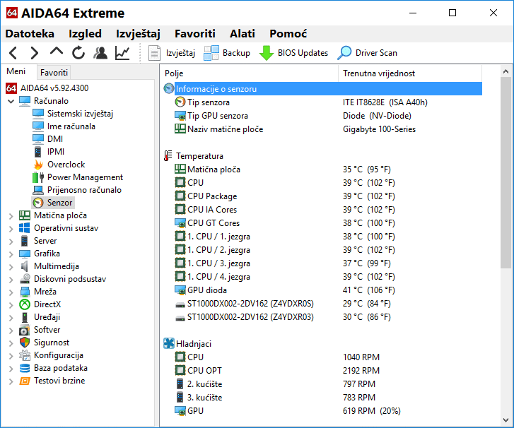 |
| Figure 4. Data provided by computer sensors for cooling. |
Of course, when you load a computer component temperatures will rise slightly, but will speed cooling fan to dramatically increase.
Between the heatsink base and the casing of the integrated circuit is smeared with a thin layer of thermally conductive paste used to overcome the impact of prominence between the surfaces. Contact surfaces can be the purpose of better mutual seating polished. Integrated circuits are designed to operate during normal usage in the TEMPERATURE range of 0°C to +55°C, while for military purposes that range is from -15°C to +70°C. This applies to circuits that are made on the basis of silicon, which is currently the case for most of them. Beyond the scope of this circuitry is not functioning or will be damaged. It is not surprising that areas with key network devices and computers conditioned. And for the same reason and the inside spacecraft is air-conditioned and people are not the primary factor :-). One recalls that the computer casing should be well ventilated. You should periodically clean accumulated dust and rib of cooling components.
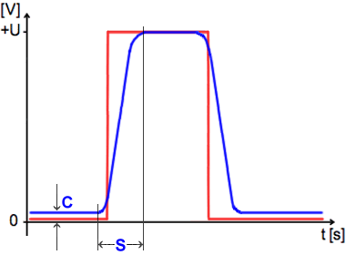
Why transistors heat when 'work' in the area of conducting or non-conducting power switch as shown in Figure 1.2.1? The reason is the time it takes to switch the transistor from the state of conducting current state to state of not-conducting current (position S in the figure), and vice versa, as well as the lowest voltage necessary to maintain current conduction (position C in the figure), as shown by the blue curve in the following figure compared the ideal curve red.
 |

|
| Figure 5. Voltage conditions of transistor. |
The general formula for power is P=U•I, and the energy is developed power in time. So, if the transistor is not flowing current (I=0), no energy is consumed or released heat. When turn the transistor current flows, as is the case in the period of time during the transition from the state of transistor of not-conducting the current state of conducting and minimal presence of current and voltage in a state of conducting, it is clear that in these two cases is developed a power consumption (I≠0, U≠0) which is part of the converted heat.
From the above it is clear that the higher the speed of the chip, has the effect of each of its individual transistors greater number of changes in the operating unit of time and thus more heat. What is more elementary transistors chip heating is higher. Accordingly, the developers try to use contemporary technologies to reduce transition time to and voltage required to maintain the state of conducting. Duration of the transition state is highly correlated with the size of the elementary transistor - a transistor less time 'flyby' electrons from one electrode to the other is a shorter, and therefore less heat.
Not so long ago, when the account was high and the speed of the computer components was not a factor, the notion of the cooling system was of no importance. Rarely had that chip cooling system. But it is because the entire room where the computer was air-conditioned. But today computers are much smaller, standing at the table, or a table of users in a dedicated inclosure. A component inside the case to cool down. In order to achieve better performance, today is the absence of any cooling system on the key components of a personal computer system unthinkable.
Back in 1983, IBM (Big Blue) introduced the IBM PC-XT personal computer, and a year later an improved version of the IBM PC-AT. What makes them 'big' is the free license for anyone who wants to deal with PCs. Now the first in the world have managed to produce a semiconductor chip in 2 nm technology, making transistors in the chips smaller than ever before. Thus, such chips are more energy efficient and enable far better device performance. It is worth watching the next video they released on May 6, 2021.

|
| Figure 6. IBM - 2 nm technology. |
IBM says it won't take too long for 2 nm transistors to become an new industry standard of semiconductor technology. It seems that the 'Big Blue' will offer the world a free license to produce chips in new technology and once again make a revolution in the world of electronics. It seems that everything I have written on this site is becoming history.
SUMMARY:
However, not everything is so simple regarding the production of a 'large thin cake' (wafer), viewed through the history of the development of machines for the production of semiconductor circuits. Everything was much simpler at the time when transistor technology prevailed, when the development of chips was still in its infancy. Almost every country had multiple manufacturers of semiconductor components, but as the criteria for the development of semiconductor components increased, especially integrated circuits, so did the price of the devices they could produce, causing all the 'small' ones to fail. Now there are only two companies in the world that are able to produce modern integrated circuits, namely:
The next picture shows their machine for making modern 'wafers', 300 mm in diameter.
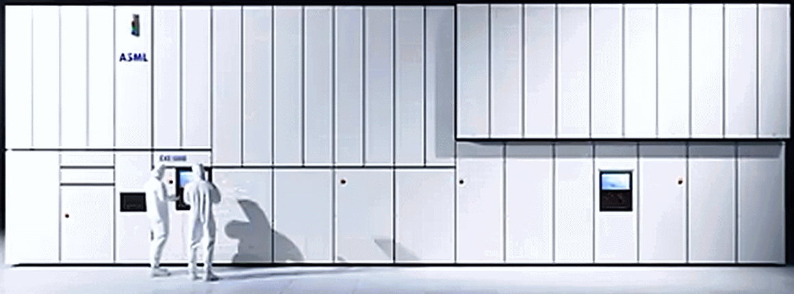 |
| Figure 7. Machine for the production of 'wafer' by ASML. |
From the picture you can see that the machine is very sophisticated, and from the cross-section you can guess that it is very complex, and therefore very expensive. They are much more sophisticated compared to F1 cars. And as today's integrated circuits are very sophisticated, and therefore in high demand on the market, whoever owns a machine for their production has a great technological advantage over others. Therefore Dutch government placed restrictions on chip exports in order to protect national security. This measure affected ASML as one of the most important companies in the global microchip supply chain. Export license requirements came into effect in September 2023.
The contributions of ASML and TSMC in semiconductor chip production have been instrumental in shaping the global technology landscape. ASML's lithography systems, particularly EUV technology (Extreme Ultraviolet Lithography), have revolutionized chip manufacturing, enabling the production of smaller and more advanced chips. TSMC's leadership as the largest independent semiconductor 'foundry', combined with their focus on advanced process technologies, collaborative partnerships, and sustainability, has propelled the industry forward.
Definitely, the technological development of semiconductors is a very expensive and a scary investment. Therefore, recent events are not surprising. As the risk of a war between Taiwan and the People's Republic of China increases, TSMC and its investors have explored options to mitigate the consequences of such an event. Since the beginning of the 2020s, TSMC has expanded its operations outside of the island of Taiwan, opening new fabs in Japan and the United States, with further plans for expansion into Germany. In July 2020, TSMC confirmed it would halt the shipment of silicon wafers to Chinese telecommunications equipment manufacturer Huawei and its subsidiary HiSilicon. In 2020, TSMC announced a planned fabr in Phoenix, Arizona, intended to begin production by 2024 at a rate of 20'000 wafers per month. In August 2023, TSMC invested in a valuable factory in Dresden, Germany, with participation from Robert Bosch GmbH, Infineon Technologies and NXP Semiconductors and subsidies from the German government, in exchange for a 70% majority in the resulting 'European Semiconductor Manufacturing Company' (ESMC).
A technological war is clearly on the horizon and no one knows what the further course of events could be. The renewed 'Cold War', along with the conflict in Ukraine and conflicts in the Middle East, is clearly leading to an increase in negative tensions of all kinds everywhere. Not good!
|
Citing of this page: Radic, Drago. " Informatics Alphabet " Split-Croatia. {Date of access}; https://informatics.buzdo.com/specific/file. Copyright © by Drago Radic. All rights reserved. | Disclaimer |