3.3.5. Working (main) Memory |
Memory is the circuitry for memory data, a multitude of locations in which to store a certain number of bits. Element of memory that stores data of one bit is called the MEMORY ELEMENT or MEMORY CELLS.
Access to each memory cell directly by the microprocessor to the first free location discovered about writing, and therefore such a memory is called RAM (Random Access Memory), and they are done READING and WRITING of data. The first free location may not always be found on the same site. Therefore, for this type of memory used the name; random access memory.
Originally they were made mostly from memory magnetic nucleolus, small rings, tenth of a millimeter in size, which was taking in all the information on the basis of the direction of magnetization the ring. Today's semiconductor technology is fully suppressed this kind of memory.
In semiconductor technology, there are several types of memory, by function and technology of shares to:
          a.) RAM - Used to enter and read the current data and programs
                             and can be easily and quickly changed its content.
                             Content is lost (forgotten) at a power computers.
                             It is often identified by a R/W (Read/Write).
                             They are available as STATIC (SRAM) and DYNAMIC (DRAM).

          b.) ROM - Allow read-only (R/O - Read Only) already factory
                           entered data. That, after making changes to the
                           contents no longer possible, and require flawless
                           loaded content, they are very expensive and only used
                           in mass production.
                           Usually contain ASCII code and instructions
                           LANGUAGE a process or program that allows
                           enter the operating system into RAM by the inclusion
                           Computer - BOOTSTRAP program.
                           There are performance computers where the whole or
                           part operating system into the ROM. Sizes,
                           ranging from few KB to several hundred KB.

          c.) PROM - Memories like ROM. The difference is that the
                             and deleted. Charging is done for the purpose
                             devices made using a deletion exposure
                             ultraviolet and x-ray radiation. So
                             their contents can be reprogrammed.
                             Were once widespread in making the computer BIOS.

          d.) EPROM - Permanent memory that can be repeatedly recharged
                             and deleted. Charging is done for the purpose
                             devices made using a deletion exposure
                             ultraviolet and x-ray radiation. So,
                             their contents can be reprogrammed.
                             Were once widespread in making the computer BIOS.

          e.) EEROM - Specifically EEPROM, have the same properties
                               as EPROM, but erasing electrically.
                               Used for enrollment as changing system settings
                               date, time, type, and floppy disk and more.

          f.) EAROM - Their content is changing electrically, but
                               reprogramming can be done only partially.
                               Reprogramming process takes a long time.

          e.) FLASHROM - Memory that can be reprogrammed for it
                             specially written programs. Today very often
                             used to allow devices to be installed
                             an enhanced version of software (firmware)
                             e.g. BIOS, modems, CD, DVD and so on.
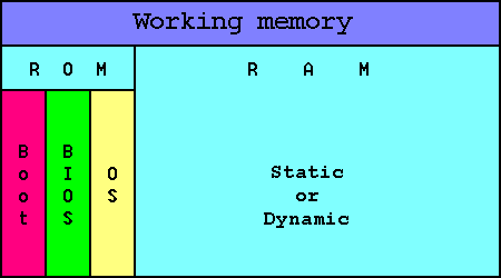
Thus, the working memory of a computer can be divided into two basic groups: ROM and RAM (Figure 3.3.9). ROM is a good deal smaller in terms of capacity of the RAM and the user is not available, only the system, and in view of the size of the data memory ROM usually not stated.
|
|
| Figure** 3.3.9 Working memory of computer. ( + / - ) |
The processor must be able to address the entire memory address space and reads the content as appropriate. Bootstrap and bios are read when you start your computer. Bootstrap are tasked by finding and connecting devices in a computer based on the data in the BIOS enable loading operating system into RAM. Some versions of the computers had been entered into the core OS ROM (Commodore Amiga) or is added to the whole OS ROM ROM (Commodore Amiga) or is added to the whole OS ROM (Sinclair ZX Spectrum), and usually reads the first sector of the drive to find a starting address of the program to load the operating system from the hard disk into RAM (LOADER). RAM is essentially a part of memory that the computer hard drive loaded with the operating system and necessary for the operation of the program and the results of the work must be in order to not be irretrievably lost, stored in non-volatile memory - basically on the hard disk.
In Figure 3.3.9c shows the part of the motherboard which shows the FlashROM memory in which they entered the program routines BIOS and bootstrap program. CMOS memory BIOS is up to ten Mbps and has a very low power consumption, and therefore can be powered with button cell. It is filled in the parameters that the BIOS reads and allows to change or adjust within a range, and use them in my work computer circuits (Electronic circuit bus, video card, drives ...). One of the parameters, for example, the date and time. In the early design of computer power CMOS and is effected by a small battery, but such a solution is replaced by cheaper button cell, CR2032 model, where the shelf life of approximately three years. After this time it is advisable to replace the battery. Software routines BIOS that first executes the POST (Power-On Self-Test) and test the attainability of the devices in the computer and the basic accuracy of communication with them. He then activates the Bootstrap. Blue jumper is used to erase the contents of CMOS and its instructions describe how to use the motherboard. CMOS memory BIOS is not part of an integrated circuit BIOS is already an integral part of some of the other circuitry on the motherboard, such as part of 'Southbridge'. Integrity of the data recorded in the CMOS is determined on the basis of registered checksums, and if the calculation of the existing data do not agree with the sum of the control that means that some of the parameters of the CMOS for some reason forcibly changed from electric shock for example.
RAM size depends on the design and entrusted to the computer and can range from a few tens of KB to the size of a few tens of GB. Working memory is a circuit that is in the nascent computer technology represent the most complex technical challenge and at cost sometimes exceeded the amount that formed all the remaining circuits together. Physical design is based on some of the CMOS (Complementary Metal Oxide Semiconductor) technology of unipolar transistors, which are basically used in all digital logic circuits and devices, from microprocessors onwards.
The difference in the performance of SRAM and DRAM is significant. SRAM takes a lot more elements and is in the process of making more expensive, but compared to DRAM but much faster and more physical. Hence it is used as a quick temporary working memory (cache) of relatively small capacity. SRAM buffer is often referred to as the interconnection between the processor and main memory. DRAM requires refresh circuitry because it works on the principle of conservation of charge, but it is slower because the lots small volume can accommodate more memory elements with much lower cost manufacturing. Therefore, the DRAM is used as the main working memory of a computer. About increased performance DRAM memory development goes in the direction of increasing access speed so that it doubles or triples clock read or write data in relation to the clock speed of the bus, DDR (Double Data Rate) technology.
The organization addressing memory locations of memory, and will depend upon the speed of data access and the speed of the system as a whole. Further examples of the basic types of memory organization, but their basic principles used in other types of memory organization which is characteristic of faster data retrieval.
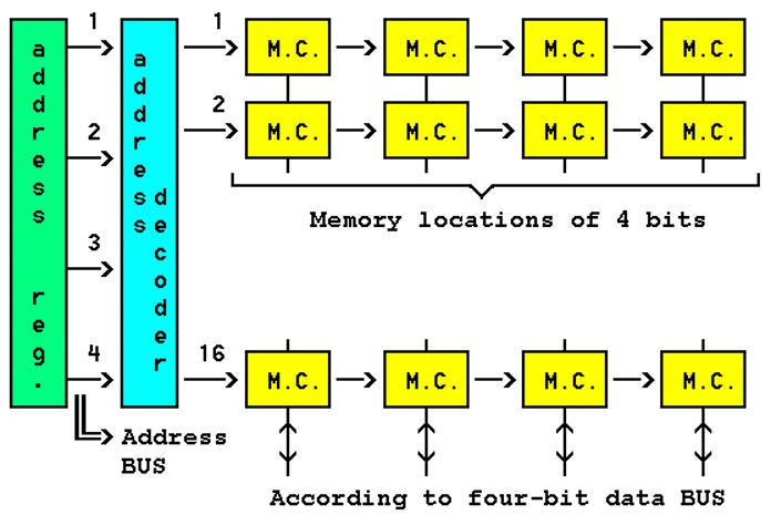
In Figure 3.3.10 shows a TWO-DIMENSIONAL organization of the working memory of the computer.
|
| Figure 3.3.10 Two-dimensional organization of memory. |
Dimensions of the memory address location and length of the site. According to this Figure of 4-bit address bus is obtained by mailing 16 different lines, each of which serves one location with 4 memory cells. For address is used only one address decoder and the unique address of the memory location.
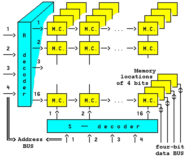
A more efficient way of organizing is when addresses are multiplexed and sent over the same address bus once given address decoder rows (R) and second column decoder (S) as shown in Figure 3.3.11.
Dimensions of the memory address line location address column location and location. Address line decoder line touring all cells that are in the line (16 × 4). The same is true for the address line column decoder. Data bus touring all locations sequentially from row to row. Address bus multiplexing, or sending of the first address line, and then addresses the column can be addressed with a total of 256 locations from 4 cells.
Instead of one decoder addresses are used with a total of two 32 an address line. Addressing 256 locations in the two-dimensional organization should be one with a decoder 256 outputs. Thus, multiplexing, not only a greater number of locations, but the total number of lines to memory network is considerably smaller, which in turn simplifies the manufacturing process.
|
| Figure 3.3.11 The three-dimensional organization of memory. |
Part of memory is organized into STACK. Stack of the most commonly used commands and operating system commands, for example, in sorting, and applications for their internal needs for storing addresses of memory locations at which he was discharged from the execution of the main program. Based on these data it is possible to again resume the main program after the cessation of executing additional actions. Therefore it is important to properly configure the system parameters stack size because otherwise get to system collapse.
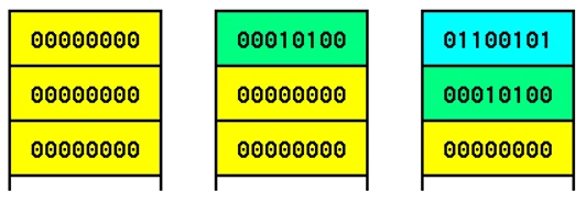
The memory is organized in the stack so that the location interrelate one 'above' and let others feed rate data recorded along the stack from the location of the site.
|
| Figure 3.3.12 Organization and feed data into the memory stack. |
Entry of new data automatically mean suppression prior to one location on. In order to achieve some sort of information 'deep' in the entire stack to stack discharge or add start address of the address decoder to mark the location stack that is active and moves to the top of the stack address.
Ideal stack no end. The principle of organization is a two-dimensional stack similar organization, except that the organization does not use two-dimensional data feed from the location of the site.
In Figure 3.3.13 shows the principle of using the data located in the memory location address of the stack with a movable top stack.
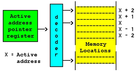 |
| Figure 3.3.13 Stack with floating point. |
The register addresses POINTER active keeps the data based on which the decoder line indicates the location that will represent the top of the active stack. Such organization of the stack is much more effective than organizations 'filling and emptying' because changing the active address stack can be accessed and data below the 'top'.
The principles of stack is not possible to organize ROM memory. However, if a stack closes the circle, access to data entered in the stack is realized by their rotation. This is therefore a circular organization of memory.
Addressing methods during program execution is closely associated with the instruction and can be carried by one of the following ways:
          1.) IMMEDIATE - When behind the location commands follow
                          bytes of program execution of a task.

          2.) DIRECTLY - By Location command follows the address where
                         to begin execution of the program task.

          3.) INDIRECTLY - By Location command followed by the address
                           at which entered starting address tasks that
                           are be executed. In fact, it is directly
                           addressing in two steps.

          4.) RELATIVE - When behind the controls is not real
                         address of the beginning of the tasks, but
                         a shift towards this address to the content
                         of the program counters that keeps the address
                         or command contents of one of the registers.

          5.) INDEXING - when similar relative to the index
                         registers (if any) keeps address of each
                         performed shift and a new shift account
                         in relation to the new address.
These are not all the possible ways of addressing. This categorization is that the most basic computer user will encounter either dealing with the set parameters of your computer and additional circuits or making the program support.
Working memory is basically used for the use of software that is kept in a permanent memory resources of the computer or computer network resources available. The working memory will be carried out primarily on the basis of data processing software execution of tasks, and store the results of the search will be a lasting memory for successively while performing tasks (a measure for example) or be saved by the execution of all tasks (for example, shading image). Thus, the size and complexity of software and the expected results will depend upon how much work and permanent memory resources should be made available in the computer. But a general rule of users of computer technology is never enough memory.
SUMMARY:
Technological development has made possible the use of computers for a very complex task. Thus, for example, image processing was almost unthinkable a PC in its first versions, and software that was developing was almost ineffective for professional use. Increase in computer power has been developing software and support and is now possible with the help of computers produced and animated sequences. Without going into the details of the image quality, it is certainly for the needy is very fast computers with high processing power, which carry enormous lot of instructions in a given time and sufficient memory resources to all sorts of frames processed.
Working memory in this regard is still fast enough and use a variety of memory organization, for example, EDO (Extended Data Out), which addresses the following line addressing location column one after another for the same target line so it essentially reduces the number of addressable lines.
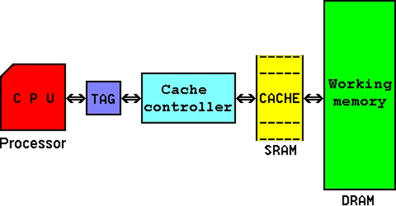
In addition to this fast SRAM memory is used for buffer (cache) between the processor and DRAM (Figure 3.3.14).
 |
|
| Figure 3.3.14 Memory organization of speed system. |
Cache controller tries to keep in the cache the more data the processor to recover from main memory. If the processor does not find the data in the fast cache controller cache memory allows him to retrieve information in working memory and sends it to him, and also stored in the clipboard as the surrounding content of information to be found the following information handy to the microprocessor in faster cache. In order to know where the data is stored in the cache memory in TAG entered his address. TAG serves as an index to the clipboard.
Cache itself runs as an integrated part of a microprocessor or a slower but larger cache on the motherboard. Of course both are many times faster than DRAM. However, the development of technology by reducing the size of transistors on elemental 22 nm, with a further reduction in its size, provided that all the stated assemblies to working memory, different levels of caching (cache) and control subsystems, to become an integral part of the microprocessor, as shown in Figure 3.5.30d. Modern microprocessors typically include more working cores organized as shown 3.5.3a, have a first level cache for instructions and data (L1) in each core, the second level cache (L2) for each core separately, and the third level cache (L3) which is common to all cores. Third level caches contains data for all nuclei including integrated graphics subsystem, which means that any data that is calculated first core, and it is the need of a third core or graphics device, available in the third level cache as a shared cache, which is used for internal distribution data (LLC - Last Level Cache) and thus functions as a kind of bus.
|
Citing of this page: Radic, Drago. " Informatics Alphabet " Split-Croatia. {Date of access}; https://informatics.buzdo.com/file. Copyright © by Drago Radic. All rights reserved. | Disclaimer |